Search This Blog

Saturday, August 20, 2011

Research in Biophotonics: Tools of the Trade

I love woodworking. Not saying that I’m great at it by any stretch, but I’ve found that in making cabinets, having the right tools makes all the difference in the world. It might be possible to find a table saw and router in the photonics center somewhere, but I haven’t seen any so far! More typically, high-level research calls for tools that are also highly technical, and which are based on science that’s not simple. To do their research, our group constructs microantennaes, like the ones shown in this image.


One thing that I found out is that the whole process involves a lot more chemistry than I would have thought. At every step, safety precautions are taken just like the ones we do at school, and more in a lot of cases. Here, they use organic solvents, and do everything under a fume hood, which is good because grad students care about their health too.


The first thing we did was to etch the pattern for our antennae using the electron beam machine. This was a lot like the process we used last year when we used photolithography to set up a design on a big silicon wafer. My friend John P. of Weymouth Physics fame did an awesome job explaining this process last year. And his blog is funny as all get out. Clean rooms will do that to people - it's gotta be the bunny suit.

After doing the first step with the e-beam machine, our chips had lots of tiny bowtie structures etched onto the surface of the wafer. The next step was to turn the outlines of bowties into things with holes in them, because the holes are key for getting light energy to go nuts in the structure.

The machine that does this is called the RIE, and it’s incredibly nasty – reactive ion etching would eat precise holes in your face if you climbed into the machine – wherever you didn’t have photoresistive material to protect you. Gas is introduced into the chamber, and it turned into a plasma by high-frequency radio waves. The plasma keeps eating silicon until you tell it to stop, so the timing of the operation is kind of a big deal.


After the RIE, we went to my favorite step – the one with the pellets of 99.999% pure gold as spray paint. Gold’s used a lot in nanotechnology for lots of reasons – it interacts really strongly with light and doesn’t react with anything in people to name two. We like it for the first reason, and to get this operation to work, we first mounted our chips upside down to the plate you can see in the picture.


Next, we put a pellet of our pretty pure gold int o a little crucible you see here. After closing down the hatch, the machine got to work creating a super-high vacuum. That took a while, but after that step, things heated up. A heating element (tungsten, I think) gradually raised the temperature to the point that the gold could vaporize.


Just like in the RIE machine, radio waves were used to excite the gold atoms, which helps them to vaporize into really tiny clusters.


At the end of the process, we had coated our bowties with gold, and they were ready for us to check out on the SEM.


In signing off for now, I would like to extend my heartfelt thanks to Serap, Ali and Prof. Altug. You were all so gracious in reaching out in the midst of your very busy schedules to teach, explain and sometimes, explain again. I know that I've gained so much understanding about what makes a research operation like this one tick - I'm sure my students and members of our school's sci-tech club will benefit. Thanks again for your support and commitment!



Monday, August 15, 2011

Research in Biophotonics: One bit at a time

When we left off, we were talking about the big picture in biophotonics, which has to do with getting the nitty-gritty information about what chemicals are doing what in disease processes. This is a tough trick because molecules are small, and because the ones we want to know about live inside of us, and not in test tubes. For the last reason particularly, Prof. Altug’s group has put a lot of effort into developing cheaper ways to build sensors that can be made cheaply, quickly and could be used not just in a lab, but also in actual living tissue.


I’ll explain a little bit about how Prof. Altug’s group is working to address these challenges, but I’d like to say two things. First, I would like to thank Serap Aksu, who always made herself available to lead the way and explain all of the many steps to the process we followed in making our sensors. Second, what I’m going to write about is research – some of this has already been published, but some if it hasn’t been yet, so I can explain in general what’s going on.

To begin with, here are a few pictures of the finished product. The bow-ties squeeze infra-red light energy into spaces that are much smaller than you could get normally. After doing some chemistry to the surface of the chip, antibodies that are designed to bond with a particular protein are added to it. Here, we’re looking at the antennae on the scanning electron microscope, which is an awesome tool by itself.

The SEM scans the surface of our finished product, gathering more scattered electrons from it when the SEM’s probe is closer to the work. In this way, the SEM can form images of very small items, and magnify things to an outrageous degree – like 500,000 X.


In the past few months, the group has created a couple of exciting developments – the first one is that they’ve perfected a system for making sensors more cheaply, and they’ve come up with ways to build sensors on soft materials, which is great, as it will enable sensors to be placed in a lot more places, like inside of us.

Next: Tools of the Trade

Friday, August 5, 2011

Research in Biophotonics: Big Picture


During the first several weeks of my RET program, I had the privilege of working on materials for the summer challenge program with our group’s research leader, Prof. Altug. This is always a great learning experience for me, and the chance to get to see her perception of developments within the field of photonics is invaluable – it’s really like being on safari with an expert guide. In the latter half of my time there, I got to be involved with the research end of the business, and was able to get to know a couple of graduate student members of her team as I participated in their research. Here, Alp checks out the result of some work he's done on his chips, while Serap waits to check on hers.


If you’ve followed the last entry about beating the diffraction problem, then you know that one of the keys to ultrasensitive detection of molecules is to focus light right where it needs to be. To do this, members of the Altug group, like Alp and Serap, have tried out many different designs for tiny antennae that can work this particular magic. Participating in this process was really educational on a couple of levels. Most importantly, everyone that I spent time with works incredibly hard at understanding each step of what they’re doing. Building and testing these tiny devices takes a few days at least, and everything is done along each step of the way to verify what’s been done. What I saw first-hand was a great example of how science really works - anyone who would ever doubt the honesty or ability of the people that I worked with just hasn’t seen these folks work up close.

So here’s the big picture: right now, screening for diseases like Alzheimer’s, Parkinson’s and many cancers is a hit and miss kind of deal. For example, breast cancer screens may miss what’s going on as much as 10% of the time. While there are some amazing new medicines out there right now that can work if the diseases are caught early, the tests that will tell you if you have the disease are still expensive and don’t work that well. The trick then, is to find which molecules will definitely mean that a particular disease is present or isn’t present.

Here’s a brand new one that seems to work: Alzheimer’s disease seems to be closely tied with a particular protein. In order to understand how the disease is working, what researchers would like to do would be to get sensing equipment actually inside of people who are developing the disease. That way, we’ll be able to really peel apart how the disease is operating, and know for certain if the biomarker is a clear indicator. And that’s another big aspect of Prof. Altug’s research – building better sensors so that researchers can speed up and improve their quest to exactly pinpoint the chemicals that are doing the dirty work in some of the nastiest diseases human beings can get.


Next: One little slice of the pie.

Monday, August 1, 2011

Summer Challenge!

Summer Challenge!

Providing clean water, ample food, high-quality medical care and education to people around the world are a few of the challenges facing the global community today. We know that when these things are in place, many other crucial social benefits like stable birthrates, can be achieved. Sustainability is at the heart of many of the grand engineering challenges, which I linked to in my first post this summer. One of the things that’s really significant to me about this list is that nanotechnology is going to play a significant role in achieving many of these goals. When biomedical testing can be made cheap enough that doctors can deliver the same high quality care in Boston as they can in Ghana, we will have really changed the world for the better.

Sharing this excitement was part of our challenge this summer as twenty high school students came to live at BU for two weeks, check out New England, and participate in a range of two-week mini classes. Toward the end of July, we met with our group of twenty students from San Francisco, China, Japan, New York, Texas, New Jersey, Virginia and Massachusetts to explore the basic science and new technology that is behind the developments at the Photonics Center. If you’ve followed some of my past blog posts, you have seen a lot of basic science – that light is made of small waves that bend around small things in a process called diffraction. This phenomenon is an example of super-important basic science. Here, Howard and Briana are talking through the math that explains that pattern of light on the white board, while Malika, our super undergrad engineering student looks on.


Why is it so important to understand how light and matter connect with each other? Because it’s the basis for an incredible array of new technologies – that’s why.

Take computers for an instance. As you may already know, one of the co-founders of Intel, Gordon Moore, published an observation in 1965 that became known as Moore’s Law. In that paper, Moore noticed that computer chips were becoming exponentially better, while at the same time becoming exponentially cheaper. It’s what’s behind every smart phone, every digital camera, and every other place chips find a hope, which is in almost everything we use today. However, as you might expect, there is a big problem with the idea of never-ending improvement. Today’s computer chips are smaller and faster than ever, but two things are happening.

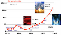
  1. is that they keep getting hotter. Like inside a nuclear reactor hot, or even hotter.
  2. is that you can only make chips so small. Today’s transistors are around 25 nm. When designers get below 10 nm, Moore and others expect that electrons simply won’t behave themselves, and chips at that size will be useless.
Boom, done, end of high-tech industry as we know it.

This is where photonics comes in. What electronics was to the 1960’s, photonics is now: an evolving field that aims to do with light what Gordon Moore and others did with electrons back then. Right now, we use fiber optics to carry information around the world, but the insides of our computers are basically 1960’s type machines. Really tuned-up, but still things that run on electrons. Today, companies like Infinera and IBM, and research universities around the country are building the technology that will enable light to carry and process information through every part of the computer. This will create computers hundreds or thousands of times faster, while using much less energy than current ones do. The Infinera link takes you to a video that demonstrates a networking chip they’ve built. It’s not a whole computer yet, but it is a big improvement on that part of the system, and the technology is a step forward. This is part of what our students learned in summer challenge, and it’s a good backdrop for the research that I did on ultrasensitive biosensing. More on that soon!